← ic 3d nano Nano dimension keyboard cover with alphabet Beschermhoes toetsenbord latexvrij vormige →
If you are searching about Disadvantages of 3D integrated circuits(3D IC) | ee-diary you've visit to the right place. We have 35 Images about Disadvantages of 3D integrated circuits(3D IC) | ee-diary like 2.5/3D IC Reliability Verification Has Come A Long Way, Southeast Asia EMS and Printed Circuit Boards Assembly News and also 2.5/3D IC Reliability Verification Has Come A Long Way. Read more:
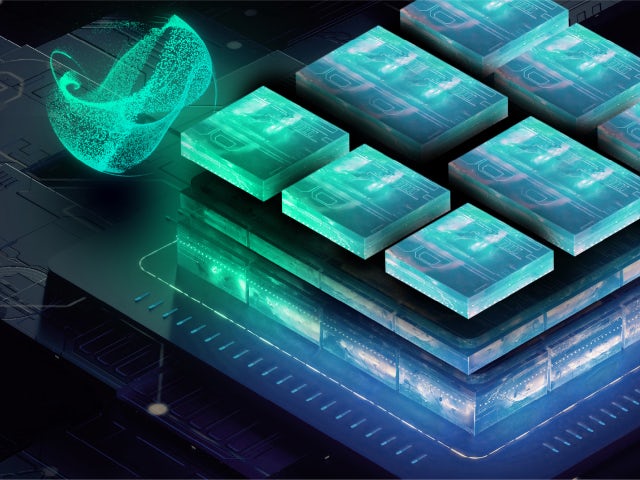
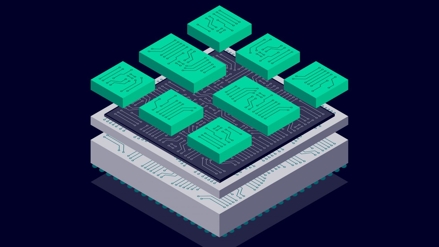
Disadvantages Of 3D Integrated Circuits(3D IC) | Ee-diary
 www.ee-diary.com
Multi-disciplinary Simulation For 2.5/3D IC Co-Design - YouTube
 www.youtube.com
ic 3d simulation
DFT Moves Up To 2.5D And 3D IC - SemiWiki
 semiwiki.com
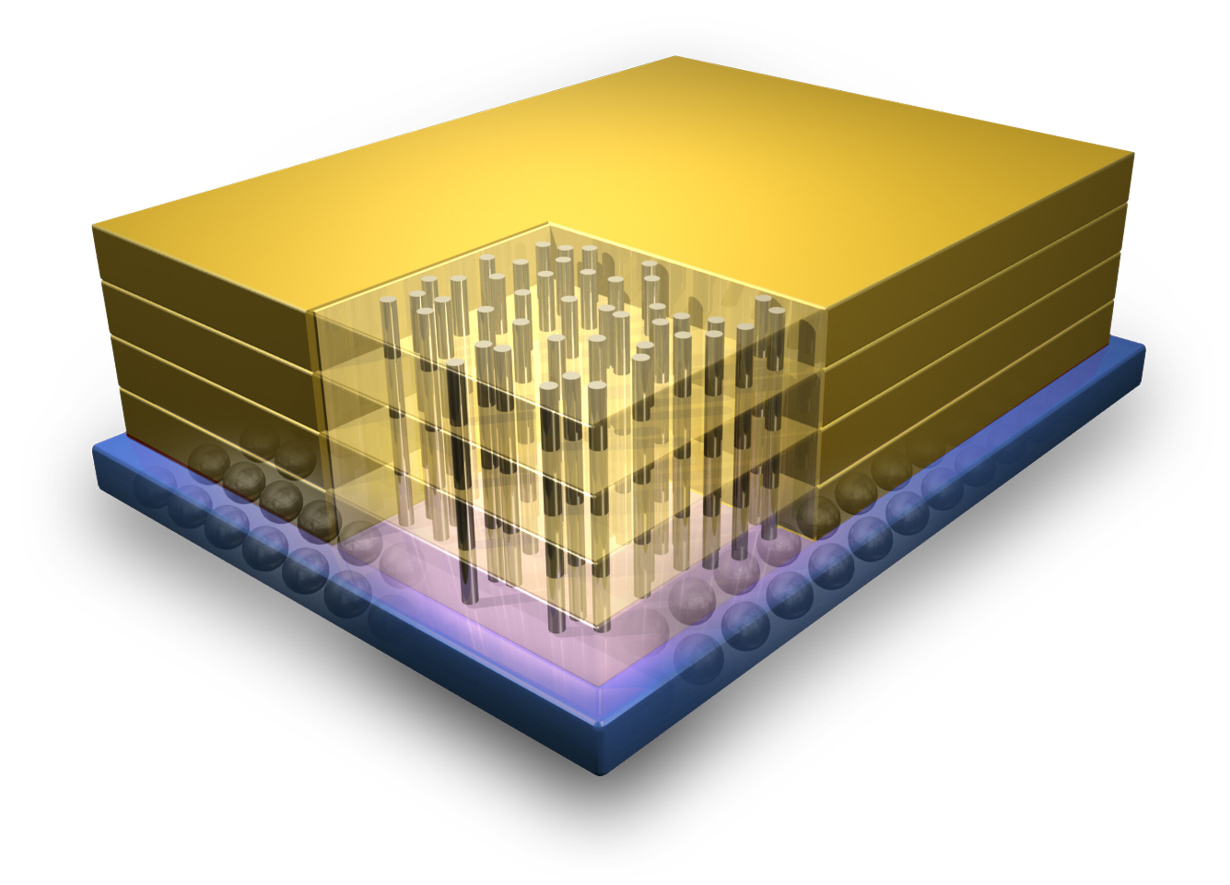
About 3D ICs | NHanced Semiconductors, Inc.
 nhanced-semi.com
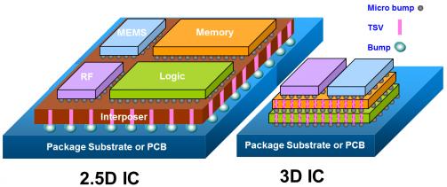
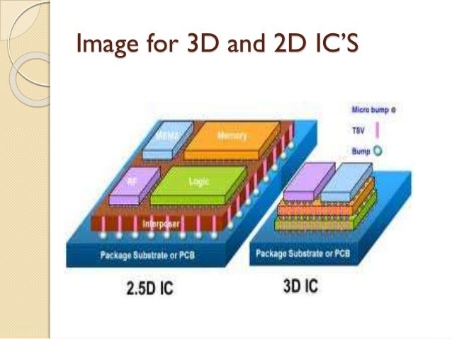
3d ics technology compared provide several 2d traditional architecture
Exploring The Significance Of 3D-SOC And 3D-IC In Cutting-Edge 3D
 www.trendforce.com
3D IC Design - EE Times
 www.eetimes.com
tsvs
Increased Funds Could Catalyze TSMC’s 3D IC Research - News
 www.allaboutcircuits.com
3d ic 5d tsmc vs catalyze funds increased research example shows could courtesy used
Samsung Announces Availability Of Its Silicon-Proven 3D IC Technology
 www.semiconductor-digest.com
ic samsung silicon proven announces its semiconductor digest
Three Dimensional Integrated Circuits (3D IC) Technology By Dr. Imran
 www.youtube.com
integrated circuits
3D IC Design Guide For Semiconductor Engineers | Siemens
 resources.sw.siemens.com
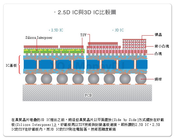
學海無涯: 先進封裝研究
 uefangsmith.blogspot.com
Advanced 3D IC Design Flow Solutions | Siemens Software | Siemens Software
 eda.sw.siemens.com
Free CAD Designs, Files & 3D Models | The GrabCAD Community Library
 grabcad.com
淺談半導體先進製程 3D封裝製程是什麼 - 大大通
 www.wpgdadatong.com
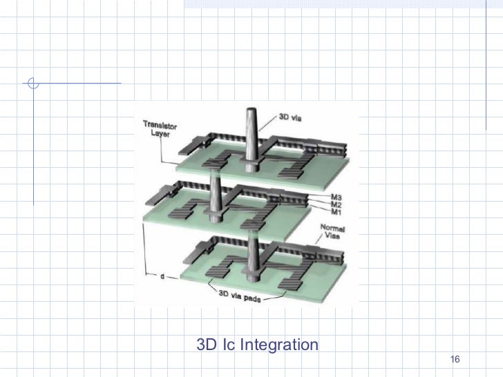
3D IC'S Technology
 www.slideshare.net
ics
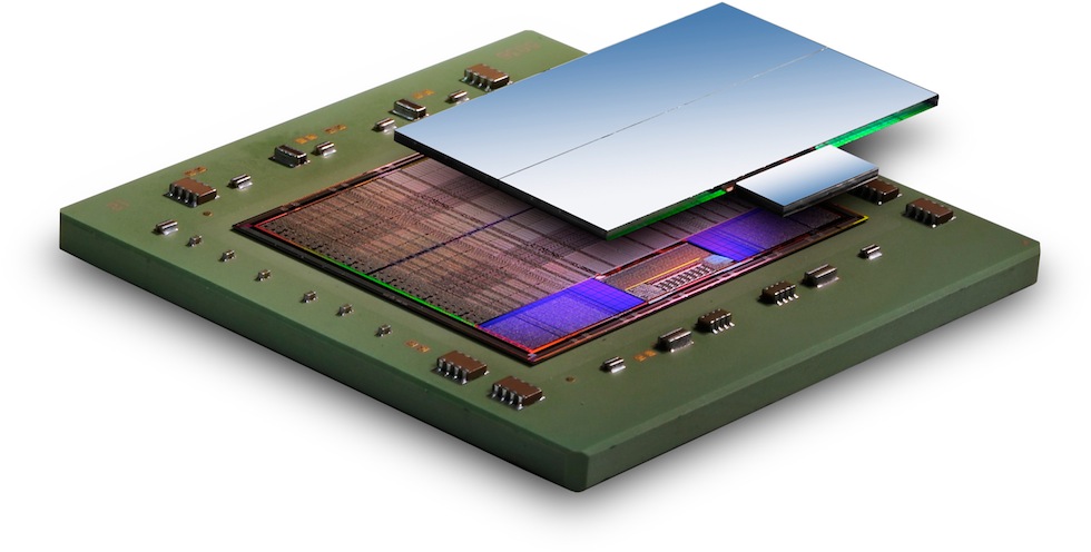
Layout Snapshots Of 2D And 3D ICs Designed In 130-nm Process
 www.researchgate.net
An Introduction To 3D IC – Ep. 1 - Siemens Software Podcast Network
 blogs.sw.siemens.com
20 GB?! Smartphones Android Com IA Integrada Precisarão De Muita
Architecting 3D Integrated Circuit Fabrics At Nanoscale - Research Outreach
 researchoutreach.org
architecting nanoscale logic nor inv combinational nand function
3D-IC Integration - Tech Design Forum
 www.techdesignforums.com
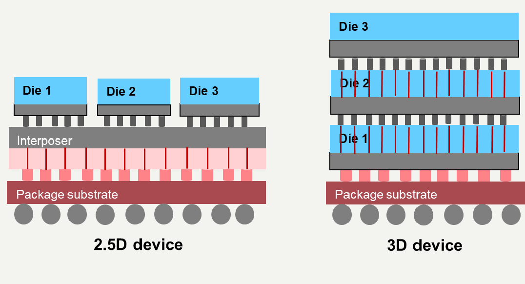
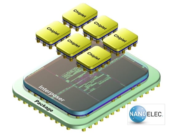
ic 3d integrated integration 5d circuits die interposer silicon chip circuit substrate 3dic stacked high xilinx demonstrated heterogenous value has
Give The People What They Want: Toward Making 3D IC Mainstream
 www.techdesignforums.com
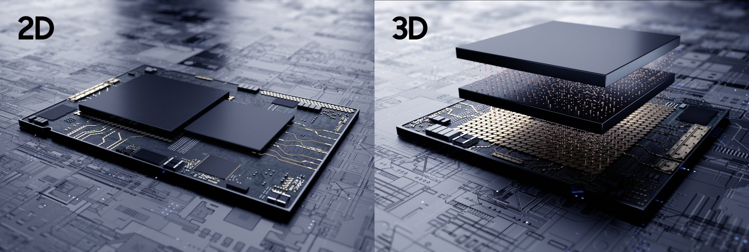
Silicon ICs Node Evolution And 2D Semiconductor Scaling Potential. A
 www.researchgate.net
Packaing Part 4 - 2.5D And 3D - YouTube
 www.youtube.com
3D ICs — Garrett Technologies, Inc.
 www.garrett-tech.com
Hypothetical 3D-IC Layout In HFSS: (a) Two Layers In Stack Of 3D-IC
 www.researchgate.net
layers stack hypothetical hfss
The Beginner’s Guide To 3D IC - Semiconductor Packaging
 blogs.sw.siemens.com
Hypothetical 3D-IC Layout In HFSS: (a) Two Layers In Stack Of 3D-IC
hfss hypothetical
Southeast Asia EMS And Printed Circuit Boards Assembly News
 globalsmtseasia.com
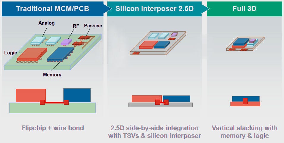
packaging advanced technology packaged 3d 5d semiconductor chips packages stack side wlp process memory shown graphic industry below
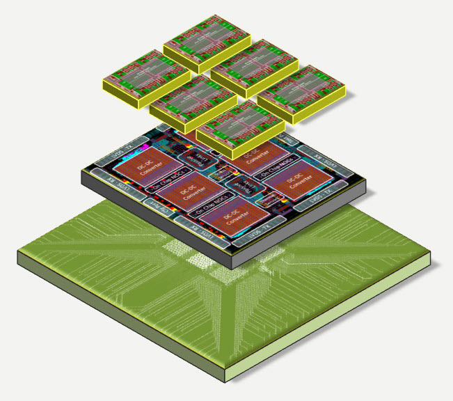
Analog In 3D ICs And Through Silicon Vias (TSVs) - Planet Analog
 www.planetanalog.com
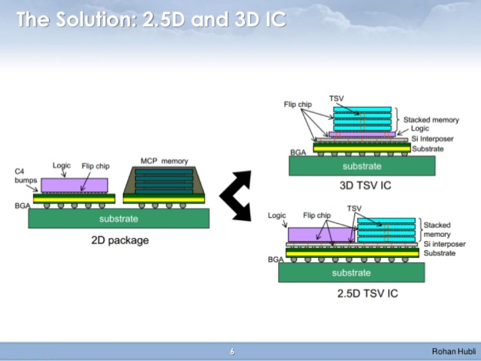
Architectural Planning Of 3D IC - SemiWiki
 semiwiki.com
3d Ic
 www.slideshare.net
IC Package Illustrations, From 2D To 3D
 semiengineering.com
2.5D And 3D ICs: New Paradigms In ASIC | By EInfochips ( An Arrow
 medium.com
Hypothetical 3D-IC Layout In HFSS: (a) Two Layers In Stack Of 3D-IC
 www.researchgate.net
stack layers hypothetical hfss 2d integrated
2.5/3D IC Reliability Verification Has Come A Long Way
 semiengineering.com
Integrated circuits. 3d ic's technology. 2.5d and 3d ics: new paradigms in asic